

WFCK is used as modulator for the logic 1 in the modchip injection routine. To generate a 1, the chip toggles between 0 and 1 at the WFCK frequency. This is supposed to fool the tracking error analog circuit to see a 1.
It is still unknown today whether the modulator can be some other signal, or if it has to be WFCK.
I guess we now know at least one other signal that can be used.
Maybe that DA07 switches at the same frequency as WFCK?
(WFCK = word clock or some such)
PSNee further development
-
postal2201
- Curious PSXDEV User

- Posts: 19
- Joined: January 26th, 2018, 9:53 pm
Perhaps the frequencies are similar, but not the same. PsNeeV7 works very unstably with DA07. WFCK is the best choice for PsNeeV7 for all revisions of the motherboard of the PS.
As for OneChip, I'm not sure, perhaps with PM-41 (2) it's better to use DA07.
-
postal2201
- Curious PSXDEV User
- Posts: 19
- Joined: January 26th, 2018, 9:53 pm
And one more interesting scheme. An unknown chip uses BCKO instead of WFCK.

It seems this chip uses patching BIOS, but does not have the stealth mode.
It will be necessary to check with the logical analyzer what happens at these points.
It seems this chip uses patching BIOS, but does not have the stealth mode.
It will be necessary to check with the logical analyzer what happens at these points.
It's already pretty obvious that many "modulator" signals will work in place of WFCK.
Most likely, some of the alternatives would require a few timing adjustments in code.
But from a practicality standpoint, it doesn't matter much. WFCK (and others) are already available as huge test points to easily solder to.
The next best thing to achieve here is to get it to work without that signal at all
I'm starting to get more confused about the actual Data (signal injection) point though.
The IC pin it connects to is labeled "CEI", where the EI most likely means "error in", similar to "TEI" for tracking error in.
And I've seen that "C" on older PSX diagrams, always having to do with the (C)opy protection.. So hm..
-
postal2201
- Curious PSXDEV User
- Posts: 19
- Joined: January 26th, 2018, 9:53 pm
rama3, I found some information in the datasheets:
CEI - Center error amplifier input.
CEO - Center error amplifier output.
CEI - Center error amplifier input.
CEO - Center error amplifier output.
Ah yeah, I wrote what I remembered. So the C is for center..
Anyway, we know that the wobble on pressed disks creates a pattern that some kind of tracking error circuit converts to the 1's and 0's that form the SCEX string.
That error detect circuit is part of any CD DSP, but Sony added another of these for their license check.
What I'd like to know is what kind of input method produces the desired string.
To debug this on PU-22+ models, one would have to decode the SUBQ transmission that carries the "decoded" string.
But here's a thought: There's no need to actually do this on a PU-22+!
If an earlier model has the same "C" inputs, it should be possible to inject the symbols there and get the Mechacon to accept the disk as well.
The benefit: The "decoded" string is visible in clear text on the Mechacon pin 17 line. That makes it possible to test and debug other injection methods
-
postal2201
- Curious PSXDEV User
- Posts: 19
- Joined: January 26th, 2018, 9:53 pm
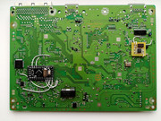
PU-18 installed
Last edited by postal2201 on April 28th, 2018, 6:13 am, edited 1 time in total.
-
TriMesh
 Verified
 - PSX Aptitude

- Posts: 230
- Joined: December 20th, 2013, 2:25 pm
- PlayStation Model: DTL-H1202
- Location: Hong Kong
On the older machines, the tracking error signal is picked off earlier in the read chain. The circuitry is basically a filter followed by an integrator followed by a comparator, and the signal is encoded by on-off keying the wobble. I'm not sure that using the same approach to fake up the signal that worked no on the PU22+ would work with that circuit.rama3 wrote: March 8th, 2018, 1:17 am Ah yeah, I wrote what I remembered. So the C is for center..
Anyway, we know that the wobble on pressed disks creates a pattern that some kind of tracking error circuit converts to the 1's and 0's that form the SCEX string.
That error detect circuit is part of any CD DSP, but Sony added another of these for their license check.
What I'd like to know is what kind of input method produces the desired string.
To debug this on PU-22+ models, one would have to decode the SUBQ transmission that carries the "decoded" string.
But here's a thought: There's no need to actually do this on a PU-22+!
If an earlier model has the same "C" inputs, it should be possible to inject the symbols there and get the Mechacon to accept the disk as well.
The benefit: The "decoded" string is visible in clear text on the Mechacon pin 17 line. That makes it possible to test and debug other injection methods
-
postal2201
- Curious PSXDEV User
- Posts: 19
- Joined: January 26th, 2018, 9:53 pm
I think these are involved in IC706. But this custom chip, datasheet is only in general terms.
There is a lot of information on the components of PU-18 with datasheets. There are also descriptions of the pin assignments of the microcircuits.
http://wiki.psxdev.ru/index.php/PU-18
There is a lot of information on the components of PU-18 with datasheets. There are also descriptions of the pin assignments of the microcircuits.
http://wiki.psxdev.ru/index.php/PU-18
-
TriMesh Verified
- PSX Aptitude
- Posts: 230
- Joined: December 20th, 2013, 2:25 pm
- PlayStation Model: DTL-H1202
- Location: Hong Kong
Yeah, the problem is that the chip in the PU18/PU20 is a semi-custom device that as far as I can see the tools and documentation never leaked for (perhaps not that surprising, since the impression I get is that they were never supplied to customers and NEC did all the detail design themselves).postal2201 wrote: March 14th, 2018, 5:30 pm I think these are involved in IC706. But this custom chip, datasheet is only in general terms.
There is a lot of information on the components of PU-18 with datasheets. There are also descriptions of the pin assignments of the microcircuits.
http://wiki.psxdev.ru/index.php/PU-18
I think a much better starting point would be the circuit used on the PU-7 and PU-8 which is built using regular components and has parts you can get datasheets for (NJM2904/NJM082B/NJM2903)

Pardon my ignorance but what's the benefit of using PSNee over Mayumi v4?
I have an Attiny85 that I could solder onto a SCPH-7501 or a SCPH-101 but I'm waiting for some PIC12F508's b/c Mayumi uses the PS1's oscillator. Is there some benefit to PSNee that I'm missing?
I have an Attiny85 that I could solder onto a SCPH-7501 or a SCPH-101 but I'm waiting for some PIC12F508's b/c Mayumi uses the PS1's oscillator. Is there some benefit to PSNee that I'm missing?
Any plans/progress on supporting the bios patch on the attiny chips?
I have a lot of other stuff going on so don't wait for me to develop this:
It may be possible to re-purpose the reset pin for an extra I/O. If you do this, and drop the serial debug output, you've got the 2 required pins.
Careful though: Once programmed, the chip can't be flashed using SPI anymore.
Only a high voltage programmer can reprogram it.
It may be possible to re-purpose the reset pin for an extra I/O. If you do this, and drop the serial debug output, you've got the 2 required pins.
Careful though: Once programmed, the chip can't be flashed using SPI anymore.
Only a high voltage programmer can reprogram it.
I did have a look at the code, and was actually thinking of using the reset and debug pins.
I don't think debug has any real purpous on the attiny anyway as I see this more like a final install, rather then a development solution.
The thing is, I see the code is in place, but i have no real experiance with microcontroller/avr programming. So i was hoping someone would pick this up. Guess i'll need an avr crashcourse.
I'm using a standalone chip programmer, so spi is no issue.
edit:
I had a quick go at a crude patch (should have checks in place for collisions between bios patching and debugging), but as a novice, I believe only some pin/port defines
should work...
fuses: LFUSE 0xE2 HFUSE 0x5F
I don't think debug has any real purpous on the attiny anyway as I see this more like a final install, rather then a development solution.
The thing is, I see the code is in place, but i have no real experiance with microcontroller/avr programming. So i was hoping someone would pick this up. Guess i'll need an avr crashcourse.
I'm using a standalone chip programmer, so spi is no issue.
edit:
I had a quick go at a crude patch (should have checks in place for collisions between bios patching and debugging), but as a novice, I believe only some pin/port defines
should work...
Code: Select all
#elif defined(ATTINY_X5) // ATtiny 25/45/85
// extras
#define USINGSOFTWARESERIAL
// board pins (Do not change. Changing pins requires adjustments to MCU I/O definitions)
#if defined(APPLY_PSONE_PAL_BIOS_PATCH)
#define BIOS_A18 3          // connect to PSOne BIOS A18 (pin 31 on that chip)
#define BIOS_D2  5          // connect to PSOne BIOS D2 (pin 15 on that chip)
#endif
#define sqck 0
#define subq 1
#define data 2
#define gate_wfck 4
//#define debugtx 3
// MCU I/O definitions
#define SUBQPORT PINB
#define SQCKBIT 0
#define SUBQBIT 1
#define GATEWFCKPORT PINB
#define DATAPORT PORTB
#define GATEWFCKBIT 4
#define DATABIT 2
#if defined(APPLY_PSONE_PAL_BIOS_PATCH)
#define BIOSPATCHPORTIN  PINB
#define BIOSPATCHPORTOUT PORTB
#define BIOSPATCHDDR     DDRB
#define BIOS_A18_BIT 3
#define BIOS_D2_BIT  5
#endif
#else
#error "Select a board!"
#endifI went ahead and compiled the code above, and am able the confirm that the TL866A/CS programmer is able to program the attiny with HVSP. So any settings to the fuses can be reverted.
unfortunately, my test PSone (SCPH-102) has a bad laser. I had to adjust the pot to even get original pal games to boot.
But, up to now, I can confirm the psone is able to boot originals, and some pal backups I had around. not sure about ntsc, as the laser was having a hard time picking up the (old) ntsc burns I have.
I was hoping my tv would output signal info like it does for hmdi, on the rgb scart input, but it doesn't. So i'm not sure the bios patch is working. If I understand correctly, it should be outputting the menu/bootscreen in pseudo NTSC..
Nice
If the patch works, the video output will indeed be NTSC 443 and the startup screen will be larger vertically.
You can try to repair your drive. Usually it needs a good cleaning and regrease with white lithium paste.
The diode itself is rarely bad (only 1 out of ~20 is worn out / my experience).
If the patch works, the video output will indeed be NTSC 443 and the startup screen will be larger vertically.
You can try to repair your drive. Usually it needs a good cleaning and regrease with white lithium paste.
The diode itself is rarely bad (only 1 out of ~20 is worn out / my experience).
Cant really trust my eyes on a 51" plasma screen. so i scoped the Vertical-sync testpin.rama3 wrote: April 17th, 2018, 12:14 pm Nice
If the patch works, the video output will indeed be NTSC 443 and the startup screen will be larger vertically.
You can try to repair your drive. Usually it needs a good cleaning and regrease with white lithium paste.
The diode itself is rarely bad (only 1 out of ~20 is worn out / my experience).
standard, it puts out 59.3Hz at bootani, and goes 50Hz at menu screen.
I insalled the tiny45 with the D2 A18 connected, and get the same thing. So it's doesn't seem te be working.
I should be getting 60Hz @ V-sync, right?
Guess it was to good to be true, needs further testing.
Last edited by Pandor on April 19th, 2018, 2:37 am, edited 1 time in total.
You should get around 60Hz, right.
Fuses look correct (using a fuse calculator).
Did you undefine (remove) #define USINGSOFTWARESERIAL ?
And did you define APPLY_PSONE_PAL_BIOS_PATCH ?
Otherwise, the code snipped looks fine with the correct pins on the correct aliases.
Fuses look correct (using a fuse calculator).
Did you undefine (remove) #define USINGSOFTWARESERIAL ?
And did you define APPLY_PSONE_PAL_BIOS_PATCH ?
Otherwise, the code snipped looks fine with the correct pins on the correct aliases.
I did not undefine USINGSOFTWARESERIAL. PSNEEDEBUG is undefined, so the serial code shouldn't execute.rama3 wrote: April 19th, 2018, 12:04 am You should get around 60Hz, right.
Fuses look correct (using a fuse calculator).
Did you undefine (remove) #define USINGSOFTWARESERIAL ?
And did you define APPLY_PSONE_PAL_BIOS_PATCH ?
Otherwise, the code snipped looks fine with the correct pins on the correct aliases.
But I did modify the code to disable TX (just to be sure it is actually disabled should i have overlook anything, and the code was actually ran.)
Code: Select all
SoftwareSerial mySerial(-1, -1); // RX, TX. (RX -1 = off)i'm on my second Tiny45 now. First time I did forget to define bios patch, and when I reprogramed it, I disabled the Reset, but Also SPI. And since the TL866 programmer only does HVSPI, i need a HVPP for that one
Maybe the delays need some tuning for the attiny.
Definitely possible, yeah.
I got the attiny port working on my sample and heard from a few others that it worked, but that's all the testing it ever got.
The BIOS patch may require a longer D2 drag down period to ensure it working.
If you still have a device to try:
delayMicroseconds(17); // max 17us for 16Mhz ATmega.. // change 17 to 15
delayMicroseconds(4); // min 2us for 16Mhz ATmega.. // change 4 to 7
If this doesn't get the patch working, then at that point someone with test gear and time will have to continue.
I have the test gear but little time..
Oh, and one more thing, because I had someone do this before:
Make sure that in your IDE, you actually compile the code for attiny45!
Who is online
Users browsing this forum: No registered users and 1 guest
 , "PlayStation",
  ,
,  , "DUALSHOCK", "Net Yaroze" and "PSone" are registered trademarks of Sony Computer Entertainment Inc.